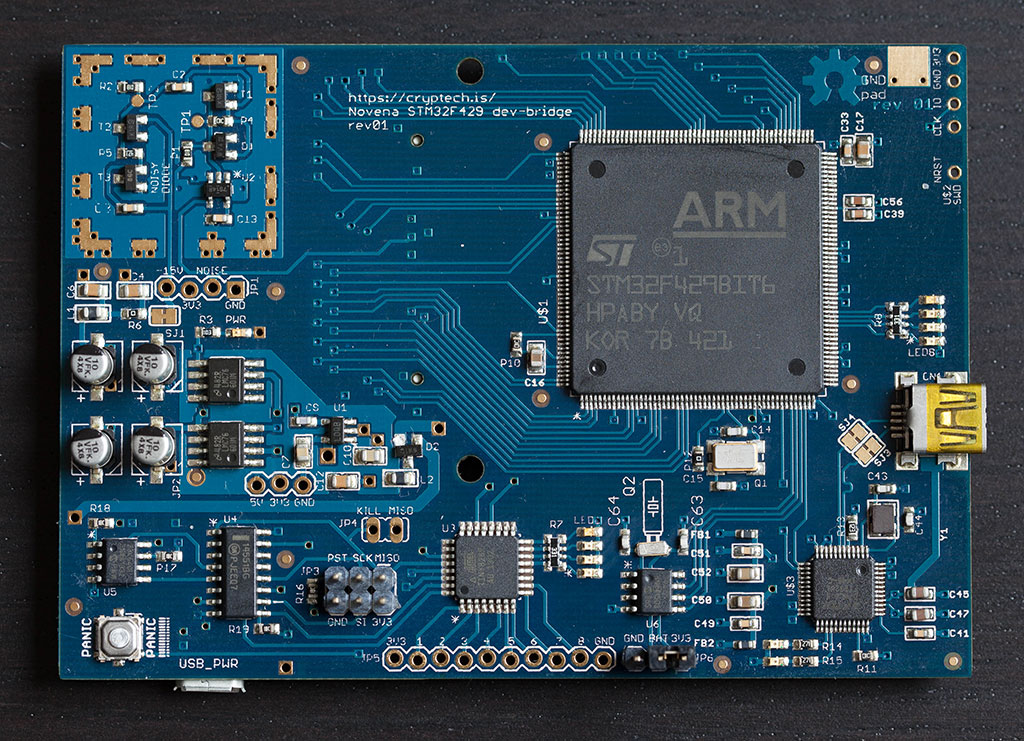
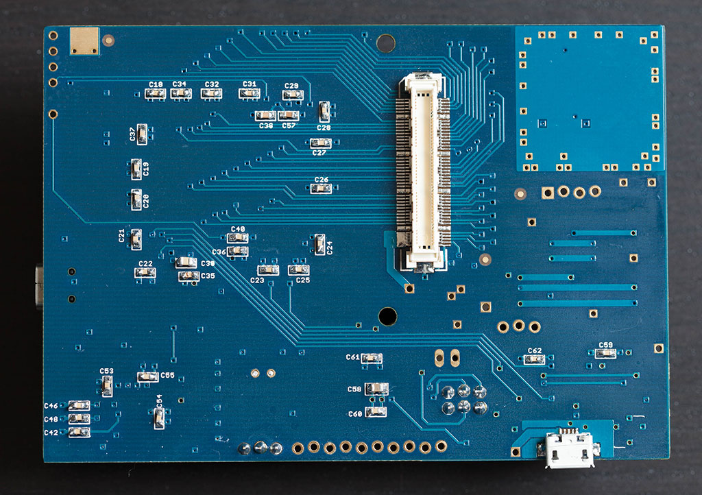
dev-bridge board
In the process of developing the AlphaBoardComponents design, the project has made what is known as the "dev-bridge board".
This is a board, 100x70 mm, with about 2/3 of the components intended to be on the Alpha design. What is missing is basically the FPGA and it's supporting circuits.
To date, the dev-bridge board has been used to implement and validate the FMC based interface that will be used to connect the ARM and the FPGA on the Alpha.
Schematics and layouts are at user/ft/stm32-dev-bridge/hardware/rev01.
High resolution pictures of rev01 of the dev-bridge board are attached at the bottom of this page, but the following should be more than sufficient to read the silkscreens.
Here is the board mounted on the Novena, attached to the programmer:
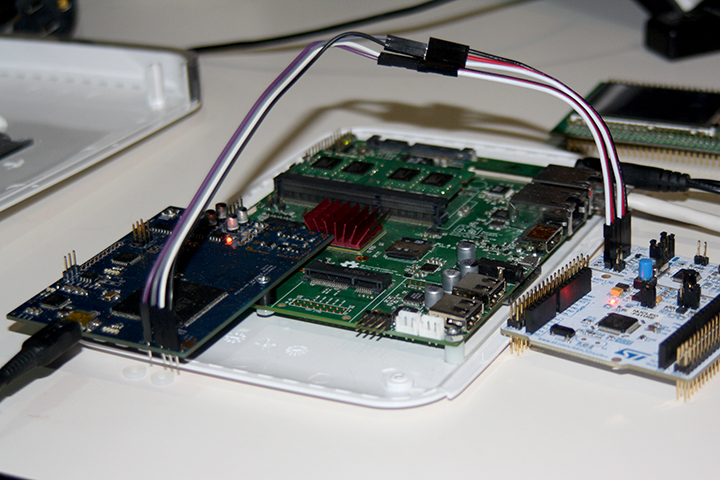
Note that it's rather bigger than the Netgear enclosure I use to transport the Novena. (Not only does it protect the board, but I have this superstition that TSA is more comfortable with a home gateway than a bare motherboard.)
Also note that the dev-bridge board is connected to the Novena by the high-speed expansion connector, which forms a bit of a pivot point. As Pavel says, "High speed and mechanical reliability are not very good friends usually."
For that reason, I highly recommend stabilizing the board by bolting it to the Novena with a 5mm spacer. There are two through-holes that line up with mounting holes on the Novena, one at the corner and one next to the wifi connector. I've found that even one bolt is enough to stabilize the board.
Finally note that the board traces come rather close to the through-holes, so you want to avoid scraping them with the bolt head or the nut. I happen to be using a countersink-head bolt, which is beveled toward the shaft, but it's probably even better to use a nylon washer.
All the software, as well as flashing instructions, are at sw/stm32.