How to start using coretest_hashes on the TerasIC C5G Board
This is a writeup on how to setup, build and testrun the coretest_hashes
Cryptech subsystem on a TerasiC C5G Cyclone V GX Starter Kit FPGA
development board 1.
Introduction
Test Setup
The test setup consists of:
-
A development computer running the Altera Quartus II FPGA development software. This computer will be building the FPGA comfiguration image (a sof-file) and then use the Altera USB-blaster to load the image into the FPGA on the TerasIC board. This computer shall therefore be connected to the USB-blaster port on the TerasIC board.
-
A host computer that runs the
hash_testerapplication that communicates with the FPGA design downloaded into the FPGA and perform tests on the hash functions. The host computer is connected to the USB-serial port on the TerasIC board. -
The TerasIC Cyclone 5 GX Starter Kit (C5G) board.
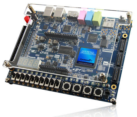
The TerasIC Cyclone 5 GX Starter Kit board.
The USB ports are the shown in the upper left corner. These are USB type B ports. The port to the left is the USB-blaster port. The port to the right is the USB-serial port. In the bottom right corner there is a row of buttons and just above them 8 LEDs. These will also be used by the coretest_hashes subsystem. There is a HDMI port on the C5G board but it will not be used. All communication is done in CLI on the host computer.
NOTE: You don't actually need two separate computers. You can use one computer with one or two USB ports. If you only have one USB port you will need to switch from connecting to the USB-Blaster port to the USB-serial port on the C5G board once the coretest_hashes FPGA configuration has been downloaded to the board.
My personal setup is a laptop with two USB ports which allows me to have connections to both USB ports on the C5G boards simultaneously.
Coretest_hashes
The coretest_hashes is a subsystem that is a FPGA design that contains Cryptech application cores as well as support cores used to run tests of the
SHA-1 and SHA-256 hash functions from a host computer via a serial
interface connected to a FPGA device. The subsystem consists of:
-
sha1: A HW implementation of the SHA-1 hash function.
-
sha56: A HW implementation of the SHA-256 hash function.
-
coretest: A command parser that accepts read/write commands from a host, executes the commands and sends the response.
-
uart: A simple serial interface that connects coretest to the host.
-
coretest_hashes: A top level wrapper that connects all the cores as well as connecting the rxd and txd ports on the uart to external pins as well as clk and reset. This core repo also contains the Python command line programhash_testerwe will be using to talk to coretester and perform tests of the sha1 and sha256 cores.
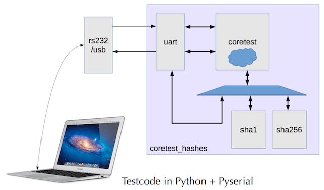
The coretest_hashes subsystem with sha1 and sha256 cores. The system is connected to a host computer via a serial interface.
SW and system requirements
You need to download and install the Altera Quartus II Web Edition software 2. There are versions of Quartus II Web Edition for Windows and Linux. I'm using the Windows version, but Linux should work too.
You will probably also install drivers for the Altera USB-blaster in order to program the FPGA on the development board. For instructions on how to install the driver, please see the Altera page for USB-blaster 7.
For communication with the coretest_hashes in the FPGA we will be using the USB-serial device on the development board. The USB-serial chip on the
board is a FTDI FT232R 3. If your host OS does not have support for this device you will need to install drivers. For Windows the correct file to download seems to be a VCP file 7.
Finally, in order to talk to coretest_hashes from the host there is application SW. This SW is written in Python and uses the Pyserial5 library. If you don't have Python and/or Pyserial installed you will need to install that too.
NOTE: Python and Pyserial does not have to be installed in the same OS as Quartus II but can be run from a separate system and OS.
(I'm using Quartus II 13.1 64-bit version running in Win8.1 in a VM in Parallels Desktop in OX 10.9.2 during this writeup. And I use Python and Pyserial in an iTerm in OSX for the serial communication.)
With all this SW installed you should be ready to proceed to create the
coretest_hashes project.
I also recommend that you download the TerasIC C5G User Manual 4. It is a really good document that describes the boards with all functions, pins etc.
Downloading the cores
Create a project directory. I'm using test_coretest_hashes. In it I add
a core directory and a toolruns directory:
#> ls test_coretest_hashes
cores/    toolruns/
The cores we need to build the subsystem must be downloaded from the Cryptech server. The cores we need are:
sha1sha256uartcoretestcoretest_hashes
#> cd cores
#> ssh git@git.cryptech.is
hello <FOO>, this is git@cryptech running gitolite3 v3.5.2-0-g926bd5f on git 1.9.0

 R   C  [a-zA-Z0-9].*
 R W    core/coretest
 R W    core/coretest_hashes
 R W    core/coretest_test_core
 R W    core/sha1
 R W    core/sha256
 R W    core/test_core
 R W    core/uart
 R W    doc/presentations
 R      gitolite-admin
Connection to cryptech.is closed.
We can see the relevant cores and check them out one by one:
#> git clone git@git.cryptech.is:core/sha1.git
#> git clone git@git.cryptech.is:core/sha256.git
#> git clone git@git.cryptech.is:core/uart.git
#> git clone git@git.cryptech.is:core/coretest.git
#> git clone git@git.cryptech.is:core/coretest_hashes.git
We should now have a cores directory like this:
#> ls
coretest/  coretest_hashes/  sha1/  sha256/  uart/
In each of these cores there are RTL and testbenches needed to simulate and build each of them. For example the sha1 core contains:
#> cd sha1
#> ls
LICENSE.txt  README.md  src/  toolruns/
The sha1 RTL source is in src/rtl. Lets take a look:
#> cd src/rtl
#> ls
sha1.v  sha1_core.v  sha1_w_mem.v
These files are:
-
sha1.v: A top level wrapper that provides an interface to the core. In this case a 32-bit memory like interface. -
sha1_core.v: The actual SHA-1 hash function core. -
sha1_w_mem.v: The W memory including sliding window functionality used by the core.
The other cores follows a similar pattern with a top level wrapper named
<core_name>.v, the main functionality in <core_name>_core.v and then one
or more submodules.
Creating the project in Quartus
-
Start Quartus and select file/new... and select New Quartus II Project.
-
Select destination directory to be toolruns/ in your project directory.
-
Set
'coretest_hashesas name of the project -
Set
coretest_hashesas nem of the top level design entity. (Should be done automatically when entering the name of the project.) -
Press next.
-
You should now be on the 'Add Files' page. Press '...'.
-
Navigate to
test_coretest_hashes/cores/coretest/src/rtl. -
Select coretest and press 'Open'. (Note: Quartus seems to sometimes omit the .v suffix for the files depending on Windows/OS version.)
-
Back on the 'Add Files' page. Press Add to actually add coretest to the project.
-
Press '...' again and navigate to the rtl directory in
coretest_hashes. Add it like you did with coretest. -
Navigate to
test_coretest_hashes/cores/sha1/src/rtland add the filessha1,sha1_core,sha1_w_mem. This time you don't need to press 'Add' on the 'Add Files'. It is done automatically when adding more than one file at a time. -
Navigate to
test_coretest_hashes/cores/sha256/src/rtland add the filessha256,sha256_core,sha256_k_constants,sha256_w_mem. Do NOT add the filewb_sha256. This file contains an alternative top level wrapper to the one insha256.vthat instead provides a WISHBONE interface. This interface is not used in thecoretest_hashesdesign. -
Finally navigate to
test_coretest_hashes/cores/uart/src/rtland adduart,uart_core.
Back on the 'Add Files page you should now see a list of source files:
../cores/uart/src/rtl/uart_core.v
../cores/uart/src/rtl/uart.v
../cores/sha256/src/rtl/sha256_w_mem.v
../cores/sha256/src/rtl/sha256_k_constants.v
../cores/sha256/src/rtl/sha256_core.v
../cores/sha256/src/rtl/sha256.v
../cores/sha1/src/rtl/sha1_w_mem.v
../cores/sha1/src/rtl/sha1_core.v
../cores/sha1/src/rtl/sha1.v
../cores/coretest_hashes/src/rtl/coretest_hashes.v
../cores/coretest/src/rtl/coretest.v
Press 'Next' to get to the 'Family & Device Settings' page.
-
In 'Device Family', 'Family' list select 'Cyclone V (E/GX/GT/SX/SE/ST)'.
-
In 'Device Family', 'Devices' list select 'Cyclone V GX Extended Features'
-
In the 'Available Devices' list select: 5CGXFC5C6F27C7.
Press 'Finish'.
Setting up and building the FPGA design
You should now be in the main Quartus II window. In the project navigator you can see all files, open the source files etc.
You could now just press 'Start Compilation' button in the menue row (the purple play/triangle button.) This will build the complete subsystem for the type of device selected. But the generated FPGA configuration image will not map to the correct pins on the C5G board. But this build should go through without errors or warnings related to problems in the source files. It is therefore a good test to see that all files has been included.
The result from this generic build should be a FPGA configuration that uses 3666 registers, 2846 ALMs, 12 pins and can run at 88.3 MHz in worst case temperature and timing.
You now need to define the correct pins and define the clock to allow Quartus to create a FPGA configuration for our board.
All pins needed are described in the C5G manual. To save time there is
also a pin list available in the coretest_hashes directory.
-
Navigate to
test_coretest_hashes/cores/coretest_hashes/toolruns/quartus/terasic_c5g -
The file
coretest_hashes.qsfcontains assignments for a project like the one we are setting up. It contains the pin assignments. The follwing list is a slightly cleaned up version of the pin assignments:
set_location_assignment PIN_R20 -to clk
set_location_assignment PIN_P11 -to reset_n
set_location_assignment PIN_M9 -to rxd
set_location_assignment PIN_L9 -to txd
set_location_assignment PIN_L7 -to debug[0]
set_location_assignment PIN_K6 -to debug[1]
set_location_assignment PIN_D8 -to debug[2]
set_location_assignment PIN_E9 -to debug[3]
set_location_assignment PIN_A5 -to debug[4]
set_location_assignment PIN_B6 -to debug[5]
set_location_assignment PIN_H8 -to debug[6]
set_location_assignment PIN_H9 -to debug[7]
set_instance_assignment -name IO_STANDARD "3.3-V LVTTL" -to clk
set_instance_assignment -name IO_STANDARD "1.2 V" -to reset_n
set_instance_assignment -name IO_STANDARD "2.5 V" -to txd
set_instance_assignment -name IO_STANDARD "2.5 V" -to rxd
set_instance_assignment -name IO_STANDARD "2.5 V" -to debug[0]
set_instance_assignment -name IO_STANDARD "2.5 V" -to debug[1]
set_instance_assignment -name IO_STANDARD "2.5 V" -to debug[2]
set_instance_assignment -name IO_STANDARD "2.5 V" -to debug[3]
set_instance_assignment -name IO_STANDARD "2.5 V" -to debug[4]
set_instance_assignment -name IO_STANDARD "2.5 V" -to debug[5]
set_instance_assignment -name IO_STANDARD "2.5 V" -to debug[6]
set_instance_assignment -name IO_STANDARD "2.5 V" -to debug[7]
As you can see, for each pin we want to use we need to define the actual
pin in the FPGA (PIN_R20 for example) and the I/O standard the pin
should use/support.
In this design I've mapped the reset signal to the button 'KEY0' on the
board which you can find in the lower right corner. There is also a
debug port that in the coretest_hashes design is connected to the debug
port in the uart. This allows us to see byte values received by the
uart. This debug port is connected to pins that control the green LEDs
just above the row of buttons that includes 'KEY0'.
In order to enter the pin assignments select 'Assignments' in the Quartus top level menue bar. The select 'Assignment Editor'. Then either manually enter each of the assignments above. This will require two rows for each pin. For example for the clock ('clk') we would enter:
- Row 1: 'To': clk, 'Assignment name': Location, 'Value':
PIN_R20 - Row 2: 'To': clk, 'Assignment name': I/O Standard, 'Value': 3.3-V LVTTL
An easier way is to open up the file coretest_hashes.qsf in test_coretest_hashes/cores/coretest_hashes/toolruns/quartus/terasic_c5g and add the pin assignment from that file to your qsf file in test_coretest_hashes/toolruns. If you then open up the Assignments Editor the same definitions should be shown.
We now need to define the clock. Under 'Assignments' in the top level menue select 'TimeQuest Timing Analyzer Wizard'. Press 'Next' to get from the 'Intro' page.
Under 'Specify base clock settings' enter 'clk' as 'Clock Name' and 'Input Pin'. Enter '20' in 'Period' and note that 'ns' is selected as time scale. In the 'Equivalent SDC Commands' you should see:
create_clock -name "clk" -period 20.000ns [get_ports {clk}]
Now press 'Next' four times to get to the final page and then press
'Finish' to complete the clock setup. If we now look in the
test_coretest_hashes/toolruns directory there should be a file called
coretest_hashes.sdc that contains the SDC command above.
Now we are ready to build the real FPGA configuration. Press the purple 'Start Compilation' button again. After build we should now have an FPGA configuration that requires 2852 ALMs, 3666 registers, 12 pins and meets timing. The max clock frequency for the design should be about 72 MHz.
Time to load the design onto the board.
Configuring the FPGA on the C5G board
If you haven't turned on the C5G board and connected the board to the computer Quartus is installed on, do so now. You should see the 7-segment displays and LEDs start flashing in a simple sequence. This shows that the default configuration in the FPGA has been loaded and the board works.
In Quartus now locate the 'Programmer' menue button (it looks like a chip with waves). Alternatively Select 'Tools' in the top level Menue and then 'Programmer'.
In the Programmer window if everything is working magically we should
see a list view with toolruns/output_files/coretest_hashes.sof
selected. And below this list a graphic that shows a 'TDI' arrow
pointing to an Altera 5CGXFC5C6F27C7 device with a 'TDO' going out from
the device.
If the graphic is not showing (probably), you need to press 'Hardware Setup'. In the Window you should see 'USB-blaster'. If not you need to fix the drivers for the USB-blaster in your OS. If the USB-blaster is present make sure it is selected and then press 'Close'.
If the file is not showing, in the main Programmer window, select 'Add
File' and navigate and to toolruns/output_files in the project
directory. Select coretest_hashes.sof and press 'Open'.
In the main Programmer window now press 'Start' to start
programming. When this has been completed (See 'Progress' in the upper
right hand corner in the Programmer board) the LEDs etc should have
stopped blinking. We should now have coretest_hashes alive on the
development board. Time for host communication and testing!
Talking to coretest_hashes and test of SHA-1 and SHA-256
There is a (currently rather ugly) test program for
coretest_hashes. Navigate to test_coretest_hashes/cores/coretest_hashes/src/sw
#> ls
hash_tester.py
This is a Python2.x program that uses Pyserial 5 to open up a serial port and talk to coretest via the uart. The command and response format used is a very simple byte oriented format. For more info, see the README.md in the top of coretest.
The program hash_tester.py needs to know which serial interface to
use. This is defined in the main() function (yes, VERY ugly). You will
need to edit the program source to point to the serial interface
connected to the USB-serial chip on the C5G board. For me that device
is:
ser.port='/dev/cu.usbserial-A801SA6T'
If everthing is working properly you should now just have to do:
python hash_tester.py
If the communication has been set up properly you should now see:
  TC1-1: Reading name, type and version words from SHA-1 core.
  READ_OK. address 0x1000 = 0x73686131.
  READ_OK. address 0x1001 = 0x20202020.
  READ_OK. address 0x1002 = 0x302e3530.
  ...
That is the first test case that reads from specific registers in the
SHA-1 core. If we look in sha1/src/rtl/sha1.v there are some defines:
  parameter CORE_NAME0     = 32'h73686131; // "sha1"
  parameter CORE_NAME1     = 32'h20202020; // "    "
  parameter CORE_VERSION   = 32'h302e3530; // "0.50"
As we can see those hex values matches what is being read from the FPGA and is the name and version strings in the core.
Moving on, hash_tester.py also performs single block message hash tests
of both the SHA-1 and SHA-256 core. The message is "abc" padded to the
correct block size for SHA-1 and SHA-256. These tests are defined by
NIST including the expected result in 6. The block is written as a
sequence of 32-bit words to addresses mapped to the block registers in
the sha1 core.
Finally we set the init_flag in the control register in
sha1 to one which should make the sha1 core initialize and then process
the first (of possible several) message block. This takes in total 82
cycles for the core. This means that by the time the host gets the
WRITE_OK. address 0x1008. message, the core is done since many cycles
ago. We therefore check status and try to extract the digest.
Looking at the output from hash_tester.py we see:
  TC1-3: Reading SHA-1 status and digest.
  READ_OK. address 0x1009 = 0x00000003.
  READ_OK. address 0x1020 = 0xa9993e36.
  READ_OK. address 0x1021 = 0x4706816a.
  READ_OK. address 0x1022 = 0xba3e2571.
  READ_OK. address 0x1023 = 0x7850c26c.
  READ_OK. address 0x1024 = 0x9cd0d89d.
Address 0x1009 corresponds to address 0x09 in the SHA-1 core. This address contains the status of the core. 0x03 means that the data in the digest is valid and that the core is ready to accept now commnands.
The digest generated by the sha1 core is in MSB format which means that the digest generated is:
0xa9993e36 0x4706816a 0xba3e2571 0x7850c26c 0x9cd0d89d
If we compare that to the expected result in 6 we can see that this is correct. Similarly, for SHA-256 we get:
  TC2-3: Reading SHA-256 status and digest.
  READ_OK. address 0x2009 = 0x00000003.
  READ_OK. address 0x2020 = 0xba7816bf.
  READ_OK. address 0x2021 = 0x8f01cfea.
  READ_OK. address 0x2022 = 0x414140de.
  READ_OK. address 0x2023 = 0x5dae2223.
  READ_OK. address 0x2024 = 0xb00361a3.
  READ_OK. address 0x2025 = 0x96177a9c.
  READ_OK. address 0x2026 = 0xb410ff61.
  READ_OK. address 0x2027 = 0xf20015ad.
The digest generated is thus:
  0xba7816bf 0x8f01cfea 0x414140de 0x5dae2223
  0xb00361a3 0x96177a9c 0xb410ff61 0xf20015ad
Which again matches what is specified in 6
Summary
We have now set up a complete development and verification environment
for Cryptech. We have setup and built the coretest_hashes subsystem for
the TerasIC C5G board. Finally we have connected to coretest_hashes from
SW in the host and verified that we can write to and receive response
needed to perform SHA-1 and SHA-256 hash operations and get correct
digest back.
If you have not been able to complete this, please contact me (Joachim Strömbergson).
Happy Hashing!